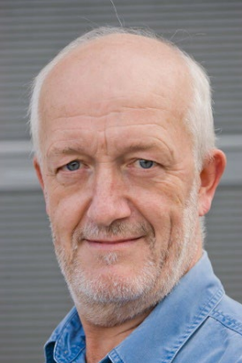
Prof. Arie den Boef
Vrije Universiteit, Amsterdam and Corporate Fellow at
ASML
Title: Image Enhancement in Optical Overlay Metrology using
Digital Holographic Microscopy
Abstract: Device density in semiconductor chips continues to increase through many innovations. For example, high-NA EUV lithography enables the printing of smaller features that allow more devices in a smaller area. In addition, many innovations are taking place in the area of 3D device integration where devices are stacked on each other.
Manufacturing state-of-the-art chips with sufficient yield requires good control of many process steps during manufacturing. Overlay, for example, is a critical parameter and describes the lateral misalignment between 2 overlapping layers in a device. Any misalignment (=overlay error) can result in a significant yield loss and overlay must therefore be controlled to the 1 nm level. These levels of control need robust overlay metrology with sub-nanometer precision levels.
Overlay is often measured on dedicated small targets using an optical microscope. However, robustly achieving sub-nanometer precision requires near-perfect imaging conditions which drives the need for high-quality high-NA imaging optics with very low aberration levels. Technically this is possible, but leads to complex and costly optical imaging systems. As a result, there is a need for a more cost-efficient microscopy technique that offers high imaging quality.
The ARCNL research institute is exploring Digital Holographic Microscopy (DHM) as a potential future option for overlay metrology. In our DHM concept we image an overlay target on a camera using low-cost high-NA optics with only a few lens elements. The resulting image is aberrated but DHM is able to computationally correct for aberrations and therefore offers near-perfect imaging in a cost-effective way.
This talk will explain in more detail the challenges in overlay metrology from an imaging perspective. We will then explain our DHM concept as a potential solution to these challenges. Experimental data will be presented that demonstrate some of these solutions. Moreover, we will also present potential solutions to some of the challenges in DHM like vibration sensitivity.
Biodata:
Arie den Boef is a Corporate Fellow at ASML where he is involved in research on optical wafer metrology. He joined ASML in 1997 and since 2016 he is also a part-time full professor at the Vrije Universiteit in Amsterdam and a part-time group leader of the “Computational Imaging” group at the Advanced Research Center for Nano Lithography in Amsterdam (ARCNL).
From 1995 till 1997 he worked at Philips Optical Storage as a System Engineer for optical recording systems. From 1992-1995 he was at Philips Medical Systems working on Magnetic Resonance Imaging. Before joining Medical Systems Arie was at Philips Research Laboratories from 1979 – 1992 where he was involved in laser diode characterization and research on optical measurement systems for industrial inspection.
Arie received a B.Sc. degree in electrical engineering in 1985 from the Eindhoven Polytechnic Institute and a Ph.D. degree in 1991 from the department of Physics from the University of Twente, The Netherlands. The topic of his Ph.D. thesis was “Scanning Force Microscopy using Optical Interferometry”.

Prof. Vittorio Murino
Istituto Italiano di Tecnologia, Italy
Title: TBA
Abstract: TBA
Biodata:

Prof. Eberhard Manske
Technische Universität Ilmenau, Germany
Title: Advanced Nanopositioning and Nanomeasuring Technology with New Capabilities for Optical Detection
Abstract: Nanomeasuring Technology is undisputedly an enabler for the acquisition of new knowledge in the nanoworld and at the same time for the implementation of nanotechnology in real applications. More and more, the limits of physics and technology are being put to the test. In particular, the fabrication of X-ray optics will not make decisive progress without high-precision nano instrumentation.
In recent years, the TU Ilmenau has succeeded in developing nanopositioning and nanomeasuring machines for a measuring range of 200 mm x 200 mm x 20 mm with a resolution of 20 pm. The enormous accuracy is only made possible by the consistent application of error-minimum measurement principles, highly accurate interferometric measurement technology in combination with highly developed measurement signal processing and comprehensive error correction algorithms.
As a remarkable result, a reproducibility of 20 pm could be achieved for length measurements in the millimeter range. The achieved relative resolution of 10-10 exceeds the potential of current conventional frequency stabilization of He-Ne lasers. Here, the first time an approach of direct coupling and stabilization of a He-Ne laser to a phase-stabilized optical frequency comb controlled by a GPS atomic clock disciplined oscillator. This enables a frequency stability of the vacuum wavelength of the He-Ne laser of 2 x 10-12 and for the first time a permanent traceability of the laser frequency to the SI unit second. Further, the coupling of the thus stabilized He-Ne laser via optical fibers with the laser interferometers of the NPM machine was demonstrated. In order to take advantage of the increased performance of the lasers in the interferometers, further work is now being done to significantly improve the stability of the refractive index within the NPM machine.
The enormous precision of the machines enables the use versatile tactile and AFM probes, as well as optical point and area sensors. Here, incredibly precise measurement results can be presented and discussed the enormous possibilities of this new technology. Finally, new approaches for further extending the accuracy of optical sensors in particular are presented.
Biodata:
From 2008 to 2013, he was spokesperson for the Collaborative Research Centre "Nanopositioning and Nanomeasuring Machines (SFB 622)" and from 2017-2020 he headed the Research Training Group "Advanced and laser-based 3D nanofabrication in extended macroscopic working areas (NanoFab)" funded by the German Research Foundation.
His research activities focus on the development of nanopositioning and nanomeasuring machines, particularly in the fields of high-precision laser interferometry, laser stabilisation, frequency comb technology, optical and tactile nanosensors and scanning probe methods. Together with Dr Denis Dontsov (SIOS Meßtechnik GmbH), he established World Interferometry Day in 1921, which is celebrated annually at the beginning of April to mark the first successful interferometer experiment by Albert Michelson in 1881.
Speakers in 2026 to be announced soon......
